![]() I figured out a way (after hearing some rumors it was possible) to through plate vias and thru holes using a liquid from a "car defroster repair kit" sold by permatex.com. I found it at Advanced Auto Parts for the cost of about 10$ US. You can also use "Silver Print" made by MG Chemicals (see update below).
I figured out a way (after hearing some rumors it was possible) to through plate vias and thru holes using a liquid from a "car defroster repair kit" sold by permatex.com. I found it at Advanced Auto Parts for the cost of about 10$ US. You can also use "Silver Print" made by MG Chemicals (see update below).
My pcb had 10 mil traces and via holes using a #72 drill. Many of the vias worked. Normal through holes like 2.54mm headers also worked, even some large holes worked. Typically the through holes were the best as they were big enough to clear the liquid through without getting clogged. However, with the vacuum table, it should suck the #72 vias fine.
First Attempt - Promising!
For my first attempt, after etching both sides of the pcb, but before drilling, I placed a large sticky label over the pcb (mine were transparent like scotch tape). I then setup my cnc machine and drilled all the holes. Using the conductive liquid from the defroster repair kit and an old glossy business card I squeegeed the liquid across the PCB over all the drill holes. I then used a vacuum on the pcb bottom side to suck the liquid through the holes. Though overall the conductive liquid stays liquid for a long time, it dries quite fast once it is spread thin. It reminds me of non-newtonian liquids such as corn starch mixed with water. This first attempt worked for about 40% of my vias but typically the liquid dried before I could get the vacuum to suck it all the way through the hole to complete the connection. Clearly, this method requires a vacuum table to suck the liquid through while it is being squeegeed.
My pcb had 10 mil traces and via holes using a #72 drill. Many of the vias worked. Normal through holes like 2.54mm headers also worked, even some large holes worked. Typically the through holes were the best as they were big enough to clear the liquid through without getting clogged. However, with the vacuum table, it should suck the #72 vias fine.
The sticker you place on the top and bottom of the PCB is of course to protect the top and bottom of the PCB from getting any conductive liquid on it. How conductive is it? Very conductive! The paper I was using as a drop cloth got soaked with the liquid and at about 5 inches the resistance was 0.002 ohms. The vias turned out to be about .015ohms, perhaps the paper had more of the liquid? Tin coating the board afterwards will probably lower the through plating impedance as well. Using the clear Avery labels I used are probably not the best choice, they are plastic based and don't drill clean but microscopically tear. Paper labels or perhaps painter's tape will work better.
Attempt 2 - Vacuum Table - 100% Success!
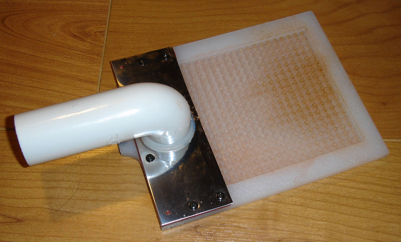
For my second attempt I built a vacuum table out of a 4$ cutting board. With my CNC machine I milled a graph pattern deep (75%) into the board. This allowed the PCB to sit on any part of the cut-out and still have lots of air circulate underneath. The graph cut-out was about 4x5 inches, I would tape over any part of the vacuum table not covered by the PCB to get a good seal so air would only be sucked through the holes in the PCB. I used plastic plumbing pipe for 4$, some sheet gasket, and sheet metal to secure an ingress vacuum port that fit my household vacuum cleaner. I tried using a compressor and two different air bed pumps too. A compressor supplies a lot of pressure but cannot provide the volume of air we need to create a good vacuum at the pcb holes. The air bed pumps were close, would probably be adequate, but the household vacuum is plenty of volume and pressure and so it the right tool for this job. The vacuum cleaner could hold the pcb to the vacuum table with quite a bit of force!
The Vacuum Table
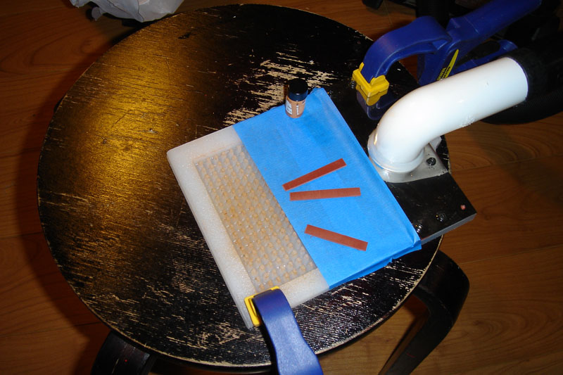
The vacuum table is made to suck the conductive liquid down through the PCB. (Click to zoom.)The table contains raised nibs so I can support small sized PCBs by sealing around the PCB with tape. Tape is used to seal areas around the PCB and the vacuum table to ensure vacuum air only through the PCB holes for maxumium amount of pressure through the PCB holes. Shown above I have blue painters tape to the size of the PCB (not shown). The small orange strips will raise the pcb slightly off the table so no holes are blocked by any part of the table.
Preparing the PCB
I used blue painter's tape to cover the pcb before drilling. The tape drilled very nicely. I am lucky to have a CNC machine that drills all the PCB holes. I only need to know the locations of two distant holes for machine alignment and therefor I don't require a full drilling template. If you don't have a CNC machine and are drilling by hand you should use paper Avery labels and print your drill or gerber artwork to use as a drill template. Since the PCB and paper is somewhat transparent held up to light, it is quite easy to align the template.
After drilling the holes I placed the PCB on the vacuum table and taped it down with more painter's tape creating a seal so the only air ingress (intake) is through the PCB holes. If you have large holes, like mounting holes, cover these with a small piece of tape while you squeegee the small holes, then remove the tape and finish the mounting holes seperately. I did about three squeegee passes for this attempt, but I probably only need 1, maybe 2. After finishing and removing the PCB from the vacuum table I placed the PCB into the toaster and baked. This will remove any remaining water from the conductive liquid and solidify it. (I should have removed the protective painter's tape first.)
There was much liquid that was sucked through and fell into the vacuum table. Clearly 3 squeegee passes was too much. I used acetate to clean the vacuum board and this worked to remove it all with very little scrubbing. It may also be possible to reconstitute this extra liquid, for a small amount of this liquid is expensive!
The results for this attempt were 100%! I only had 9 holes in this small pcb, but they were with a #78 drill (0.019in), so very small. Since I baked the board with the painters tape, I burned the tape and the adhesive became very sticky and difficult to remove from the PCB. Next time I will remove it before baking for sure! I scrubbed the sticker off with a straight edge of another pcb, a razor blade and an abrasive scotch-brite pad. The amount of abrasive scrubbing I did I am amazed the conductivity was not broken, or that water didn't reliquify the paste but after a long process of cleaning the board I still had 100% conduction! I just proved the results of this method are not flimsy. I could have used acetate to remove the adhesive but this is obviously death to the conductive liquid too. Luckily I discovered that before trying to clean the board!
Update: After visiting the permatex.com website and looking at the Material Safety Datasheet I discovered that in fact the secondary ingrediate after the dissolved silver compound is in fact acetate. So acetate would redisolve the conductuve liquid but you should also be able to reconstitute left over material by cleaning with acetate and then letting the acetate evaporate to thicken the liquid again.
Other sources of conductive liquids
Update: I am trying to track down other less expensive sources of conductive liquid. One source is from MG Chemicals called "Silver Print". The price of this stuff is around 40$ for a 1/2 Troy Ounce. This is considerably less expensive than buying in the small amount each defroster repair kit contains. This liquid works well but takes a while to dry and does not become conductive until it dries completely. Once you are done spreading this liquid in the holes, you should leave the board to sit and dry before pulling the protective tape off the board.
If you know of inexpensive sources or a way to make your own, please contact me.
Caveats
* The liquid from the defogger repair kit drys in mere seconds, too fast, when it is spread thin...so by the time I suck it with the vacuum its usually already pretty solid. Some holes seem to suck it through via capillary action (?).
* Though you can do a few holes at a time, probably better to put a good amount on and squeegee the entire board at once, the liquid stays liquid when thick so it spreads well and you dont have to rush.
* During the first attempt, some holes were clogged with liquid, some were clear. More often the clear ones work, the clogged ones don't as the liquid does not reach the bottom copper.
Problems with Conductive Fluid (new)
I've had a problem with the Silver conductive fluid recently. I used a few vias to tie the ground of my regulator to the ground plane on the bottom of the PCB. In operation, this regulator's ground pin had a tendancy to float on occasion. Perhaps it had to do with current output, I am not sure. The resistance of these vias would intermittently change upwards to 50ohms! Perhaps this plating is sufficient for small signal traces, but I am hesitent to depend on them on vias for power distribution.
There are a few other things I've noticed about the Silver fluid that suggests to me that the copper fluid is better. The silver solution takes a long time to dry and until it does it is not conductive. The copper solution dries almost too fast, but it is also almost instantly conductive. I will try the copper solution on the next board for sure.
Making the PCB
I used the toner transfer method to create the PCB. I just bought the transfer paper, the TRF foil and the TIA laminator from the guy at www.pulsarprofx.com. This method is excellent! It is so much better transfer than regular iron and tonor...the green TRF foil applied over the tonor is very resistant to abrasion and the etching process. This method can easily etch 8mil, they claim it can do 6mil with practice. Also, buy the TIA laminator for 60$, it's so worth it. My regular iron couldn't supply enough heat or pressure. The TIA lays down perfect tracks with full toner transfer and no broken traces.
I've used the photo developing method in the past. It's not as easy as the toner transfer above but I could produce very good results with practice. At the time, pulsar's toner transfer method was not available and the toner transfer method's that existed were poor for surface mount parts. One thing I learned about the photo method was rather than using transparencies, I had a Litho company produce litho transparencies for me for about 10$ (circa 1996). Regular transparencies had a lot of UV leakage within the black areas and timing the exposure was difficult. These lithos are used in exposure equipment for developing metal plates for printing presses. The exposure bulbs in this equipment are *very very* bright and so the black portions of the litho's must be super black with no leakage. With these litho's I could expose the board with UV for an hour and still not expose any part under the black. 3 minutes was more than adequate, but the point is timing the exposure was not an issue any longer.
Beyond the exposure problem, alignment of the top and bottom layer was the only thing I could mess up. Alignment still remains a difficult part of DIY PCBs when you are dealing with small via sizes like 20mil vias with 12mil holes. I hope to come up with a perfect alignment method soon too.