ColinMacKenzie.net
This is an example of a front panel interface for a digital audio recorder using a Xilinx XC9572XL CPLD interfaced with an Atmel AVR32AP7001 with the NGW100 Eval Kit. The CPLD provides "time multiplexed" sequencing for a 6 digit 7-segment LED display, 8 status LEDs, and detects input from 7 key switches generating a CPU interrupt on a key press or release. The CPLD interfaces with the AVR32AP using a simple 4-bit multiplexed bus. This provides a good example of designing a front panel interface that relieves the duty from the host CPU -- no polling!
To summarize, this controller handles:
- the display sequencing of 3x dual 7-segment LED displays (6 digits)
- the display of 8 regular status LEDs
- the input & detection of 7 switches (keys)
- bus transactions with the 32AP7001 processor over a simple 4bit (10 signal) bus
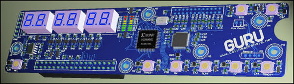
This PCB project as depicted also contains a Cirrus Logic CS4202 AC97 Codec sound chip for the AVR32AP that is not documented here.
Download Source Files
Source Files (tgz) (56.67 kB) Source Files (zip) (54.44 kB)
This file includes the Verilog source code, testbench, and output files for the controller. This source code was developed using Icarus verilog in Linux. To compile and run the testbench simply unpack the archive to an empty folder and run make. (Ensure you have the Icarus verilog compiler package installed.) The included Makefile runs the Icarus compiler and processor with the proper arguments. You should see the output from the testbench results. There is also a vcd dumpfile generated for gtkwave so you can look at the waveform timing diagrams.
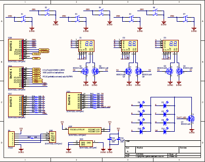
Front Panel Schematics
The controller is based on the following schematics.These schematics are part of an expansion board I built for the NGW100 evaluation kit. This expansion board provides an AC97 sound codec to the AVR32AP processor. The full schematics and PCB artwork for this expansion board will be posted at a later date. The expansion board with the ac97 codec and this front panel interface will also be available for purchase along with, (in accordance with GNU licensing,) freely available open-source code to implement a digital voice recorder using the SD card and the speex, mp3 or aac codec.
Download ac97 Front Panel Schematics as PDF
The Display Sequencer
To provide outputs from the CPLD for each of the 7 segments of each of the digits would require more pins than available on the device (48 to be exact), and would also be very ineffecient. The standard practice is to route the 7 segment pins (denoted as A-G,DP=dot) to each digit directly (daisy chain), then control the state of each digit's common cathode or ground pin. Thus even though each digit recieves the same signal, only the digit with the cathode pin active becomes visible, the cathodes on all other digits are floating or hi-impedance. (Note: some digit displays are common anode.)
To give the user the effect that all digits are being displayed at once we sequence the A-G signals and the cathode control signal very quickly, much faster than the speed of the human eye. Transistors are used between the digit's common cathode and ground to activate that digit. In my schematics I use mosfet's for low on-resistance and fast switching.
In this controller, the digit memory is 4-bits/digit. The CPU writes the value of the display via the 4-bit bus. The display sequencer has a 3-bit (0-7) counter which addresses the digit memory and outputs the stored value through a "hex to 7-segment display" decoder. This decoder takes the 4-bit input word (as hex) and converts it to the A-G signals for the 7-segment display.
Now, since we also have 8 status LEDs, why not control them with the display sequencer as well! 8 LED's cost us only 1 extra enable pin and a transistor, saving us 7 pins if we had to use 1 pin per LED. This makes our display sequencer a little more complex however, since the A-F outputs are driven by the 7-segment decoder based on only a 4-bit input. We dont want to display digit-like output on our status LEDs so the sequencer must bypass the 7-segment decoder and output 8bits directly when sequencing the status LEDs. This also means concatenating the two memory locations too, for an 8-bit value. Overall, not a major problem for our verilog program or CPLD.
The displace sequencer contains the following signals:
DISP_CLK - Input, the display sequencer clock, usually devised from system CLK, display sequences each DISP_CLK cycle.
DISPLAY[7:0] - Output, the decoded A-G+DP output to the 7-segment display.
DISP_SELECT[7:0] - Output, the select lines for the common cathode pins of digits 1-6, plus the LED status cathode enable.
The input keys
The input task is quite simple. When the CPU reads a specific memory address (the BUTTONS1 or BUTTONS2 location), we won't fetch the value from the memory but rather directly from the
switch inputs. Also, so as not to require polling by the CPU, if any switch is pressed or released we set the INTR output flag. This alerts the processor to check the BUTTONSx registers. The INTR flag is automatically reset when the CPU reads the last BUTTONS location.
If we were to have a large amount of keys we would use a switch matrix like in real keyboards and use less input pins, but for only 7 switches we can't save much.
keys[6:0] are the 7 key inputs from the signals.
The 4-bit bus
The CPU communicates with this controller over a simple 4-bit bus. This bus uses a multiplexed address/data bus. The desired read/write address is first latched into the controller using lda pin (LoaD Address). Afterwhich, one or more RD/WR strobes are used to transfer data in and out of the device. After each RD or WR cycle, the device's internal address pointer is incremented. Thus, you don't have to reload the address if you are reading or writing from/to consecutive range of memory.
We could have used a simple 2 wire bus protocol like i2c if we were really short on cpu and/or device pins. However, this would take more latches to implement, and latches are in short supply in the Xilinx 9572 parts. The 10-pin interface is pretty simple and efficient. If you have the time, another example of a common 4-bit bus is the LPC bus as used in modern motherboards and the older XBox and is a good example of an efficient 4bit multiplexed bus! The LPC bus reduces the old ISA bus to about 10 pins without sacrifices in speed or features.
The 4-bit bus has the following signals:
CLK - Input, The bus clock
RST - Input, Resets the device
DA[3:0] - Bidirectional, The 4-bit multiplexed address/data bus
RD - Input, Active low during a read cycle
WR - Input, Active low during a write cycle
LDA - Input, Active low to latch DA[3:0] into the device's internal address latch register
INTR - Output, goes low when a key is pressed or released until the CPU reads the BUTTONS1 register
Memory Map
The following map outlines the registers internal to the device and thier read/write access.
00 R/W: DIGIT 001 R/W: DIGIT 1
02 R/W: DIGIT 2
03 R/W: DIGIT 3
04 R/W: DIGIT 4
05 R/W: DIGIT 5
06 R/W: Status LEDs 4-7
07 R/W: Status LEDs 3-0
08 R/W: DP2 5-4 7-Segment Display Dots
09 R/W: DP1 3-0 7-Segment Display Dots
0a R: BUTTONS 6-4
0b R: BUTTONS 3-0
Timing
Each step in the following timing diagrams is a cycle of the CLK. You can safely have many clock cycles occur for each step (relaxed timing requirements), but you must have at least one.
Writing to memory
1: Set da to the 4-bit memory address, set lda low2: Set lda high, set da to data value, set wr low
3: Set wr high
[ if we wish to continue writing in the next memory location, we repeat ]
4: Set da to data value, set wr low
5: set wr high
[ repeat from step 4 for more data ]
Reading from memory
1: Set da to the 4-bit memory address, set lda low
2: Set lda high, set rd low
3: Read data from da, set rd high
[ if we wish to continue reading from the next memory location, we repeat ]
4: Set rd low
5: Read data from da, set rd high
[ repeat from step 4 for more data ]
Timing Diagram
See the Source Files Archive for larger timing diagram and a GTKWave save file and VCD file for more in depth look at the timing sequences.
In this diagram the top 5 rows represent the Display Sequencer output. "display-translated" is the same signals as the "display[7:0]" signals, only it is translated by GTKWave using a translation filter file. This translation filter file translates the 7-segment output back into hex value including the DP (decimal point).

Using Icarus Verilog
I would like to take a moment to speak about Icarus verilog, the free open-source verilog compiler. At first glance I had some problems using Icarus, mostly due to not having a convenient GUI to use with debug and waveform windows. I've used ModelSim previously but this package is expensive and doesn't provide an easy way for beginners to download and try out my code. My goals in posting my verilog/HDL projects here is to get more people interested and working with Hardware Descriptive Languages as I believe certain problems are best solved in programmable logic. Furthermore, programming programmable logic devices are so much easier now-a-days than ever before, no good systems engineer should feel shy to use them. For this reason, I resolved to using Icarus Verilog for every project I will post online.
Now that I have become more fluent in writing my test benches and using the simulation/debug functions provided by verilog, coupled with a Makefile, I find writing modules with Icarus very quick and easy now, and just as quick as with ModelSim. So have no fear, just like Icarus, fly close to the sun...and soon you'll make it over the Icarus humps.
Icarus also isn't fully Verilog2001 compliant. It is missing a few features like the generate statement and bit-level accessing of word memory arrays. Both of these features could simply a bit of the following code, but in synthesis it probably wouldn't make much of a difference in latch/routing resources.
Verilog Source Code
module ac97ui(
clk, rst, da, rd, wr, lda, intr, // 4-bit bus interface
disp_clk, display, disp_select, // display ports
keys
);
input clk, rst, rd, wr, lda; // our system clock
output intr; // interrupt output when a key is pressed or released
inout [3:0] da; // bidirectional address/data bus
input disp_clk; // seperate display clock
output [7:0] display; // the decoded 7-segment display output
output [7:0] disp_select; // disp_select decoder decodes only when data is not 0xf
// the keys/buttons, our input switches
input [6:0] keys;
// the names of each of our address locations
parameter D0 = 4'b0000; // Digit 0
parameter D1 = 4'b0001;
parameter D2 = 4'b0010;
parameter D3 = 4'b0011;
parameter D4 = 4'b0100;
parameter D5 = 4'b0101;
parameter LEDS2 = 4'b0110; // Status LEDs [7:4]
parameter LEDS1 = 4'b0111; // Status LEDs [3:0]
parameter DP2 = 4'b1000; // Digit Dots [5:4] (bits 6,7 are dont matter)
parameter DP1 = 4'b1001; // Digit Dots [3:0]
parameter BUTTONS2 = 4'b1010; // Buttons [6:4] (bit 7 always reads as 1)
parameter BUTTONS1 = 4'b1011; // Buttons [3:0]
// our memory core consisting of Instruction Memory, Register File and an ALU working (W) register
reg [ 3:0 ] addr; // our address register
reg [ 3:0 ] mem[7:0] ; // our digit memory
reg [ 5:0 ] dpmem; // memory for our display dots (must be seperate memory because of icarus verilog bit-select limitation)
reg intr = 1; // active low when a key is pressed
reg [ 2:0 ] disp_addr;
wire [ 3:0 ] digit; // the value of the addressed hex digit
wire [ 6:0 ] hexdecoder_out;
wire dp_out; // our dot value for the currently sequenced digit
// instantiate our hex to 7 segment decoder
hex_to_7segment hexdecoder( digit, hexdecoder_out );
// this task resets our device
task dev_reset;
begin
{mem[0],mem[1],mem[2],mem[3],mem[4],mem[5],mem[6],mem[7]} = 32'b0;
dpmem = 6'b000000;
intr = 1;
addr = 4'b0000;
disp_addr = 4'h00;
end
endtask
// the initial state, not synthesized, so a reset cycle is recommended/required
initial #1 begin // reset on second timestep
dev_reset;
end
/* 4-bit Simple Bus
*/
// during a read, we get the value from memory or directly from the switches
assign da =
(rd) ? 8'bz :
(addr==DP2) ? {2'b11, dpmem[5:4]} :
(addr==DP1) ? dpmem[3:0] :
(addr==BUTTONS2) ? { 1'b1, keys[6:4] } :
(addr==BUTTONS1) ? keys[3:0] :
mem[ addr ];
// at each clock cycle we manage the state of the 4bit bus
always @ (clk, rst)
begin
if(!rst)
dev_reset; // keep the device in the reset state
else
begin
if(!lda)
addr <= da; // address load operation
else if(!wr)
begin
// if addr is DP2 or DP1 we set our dot memory
if(addr==DP2)
dpmem[5:4] = da[1:0];
else if(addr==DP1)
dpmem[3:0] = da;
else
mem[ addr ] <= da; // write contents of da bus to digit memory
end
else if(!rd && (addr==BUTTONS1))
intr = 1; // a read of the buttons location occured, clear the interrupt flag
end
end
// auto increment the address register after every read/write operation
always @ (posedge wr, posedge rd)
addr <= addr + 1'b1;
/* display sequencer
*/
// assign the input to our hex decoder from the addressed memory
assign digit = mem[disp_addr];
// assign the hex decoder output to the display out, unless we are addresses the LEDs then output the values directly
assign display = (disp_addr[2:1]==2'b11) ? {mem[LEDS2],mem[LEDS1]} : {dp_out, hexdecoder_out};
// decode the display address to digit select pin (a digit value of 0xf value means no display output)
assign disp_select =
(digit == 4'b1111) ? 8'b00000000 :
(disp_addr == 3'b000) ? 8'b00000001 :
(disp_addr == 3'b001) ? 8'b00000010 :
(disp_addr == 3'b010) ? 8'b00000100 :
(disp_addr == 3'b011) ? 8'b00001000 :
(disp_addr == 3'b100) ? 8'b00010000 :
(disp_addr == 3'b101) ? 8'b00100000 :
(disp_addr == 3'b110) ? 8'b01000000 :
(disp_addr == 3'b111) ? 8'b10000000 : 8'b00000000;
// fetch the dot from memory
assign dp_out = dpmem[ disp_addr ];
// increment the digit address each display clock
always @ (posedge disp_clk)
disp_addr = disp_addr + 1'b1;
/* Input Key Detector
*/
// key detector
always #1 @ (keys) // #1 schedule prevents interrupt on simulation startup (not synthesized)
intr = 0;
endmodule
Sample Testbench Output
guru@yogi:~/projects/ac97-frontpanel$ makecompiling...
VCD info: dumpfile ac97.vcd opened for output.
Testing bus interface for proper reading/writing:
writing digits.
writing status LEDs.
writing dots.
reading digits:
digit 0: f
digit 1: 2
digit 2: 4
digit 3: 5
digit 4: 8
digit 5: 1
LEDs: 01101001
dots: 11101011
buttons: 11111111
pressing a button:
interrupt at time=70
buttons: 11111011
releasing button:
interrupt at time=90
buttons: 11111111
pressing a button:
interrupt at time=100
buttons: 11011111
releasing button:
interrupt at time=120
buttons: 11111111
// 0x00000000
1
6
3
9
7
0
6
9
Hex to 7-Segment Display Decoder
Our digit memory is stored as 4-bit hexadecimal values, thus to output to the 7-segment display we require a decoder. The decoder is entirely combinational and doesn't require any latches.It converts our 4-bit value into a 7-bit value representing the activated segments of the display.
module hex_to_7segment(
in,
out
);
input [3:0] in; // our system clock
output [6:0] out;
// the names of each segment and its bit output
parameter A = 7'b0000001;
parameter B = 7'b0000010;
parameter C = 7'b0000100;
parameter D = 7'b0001000;
parameter E = 7'b0010000;
parameter F = 7'b0100000;
parameter G = 7'b1000000;
// combine segment to output the digit (it'so easy!)
assign out =
(in == 4'h0) ? A|B|C|D|E|F :
(in == 4'h1) ? B|C :
(in == 4'h2) ? A|B|G|E|D :
(in == 4'h3) ? A|B|C|D|G :
(in == 4'h4) ? F|B|G|C :
(in == 4'h5) ? A|F|G|C|D :
(in == 4'h6) ? A|F|G|C|D|E :
(in == 4'h7) ? A|B|C :
(in == 4'h8) ? A|B|C|D|E|F|G :
(in == 4'h9) ? A|B|C|D|F|G :
(in == 4'ha) ? A|F|B|G|E|C :
(in == 4'hb) ? F|G|C|D|E :
(in == 4'hc) ? G|E|D :
(in == 4'hd) ? B|C|G|E|D :
(in == 4'he) ? A|F|G|E|D :
(in == 4'hf) ? A|F|G|E :
4'bz;
endmodule
TestBench
The first thing I do when creating a new verilog file is to create the Testbench. This file provides test stimulus signals to our module purely for simulation (and therefor is typically not synthesizable). I find writing the testbench first prepares myself for the behavior of the actual module.
In this testbench I wrote three functions (tasks actually) that handle the bus communication, ac97_ldaddr(addr), ac97_write(data), ac97_read(data). The ac97 first loads a desired address into the internal address latch of the CPLD. One or more read or write functions can then follow. The address latch will automatically increment after each read or write allowing for a range of memory locations to be read or written efficiently.
module tb ();
reg clk, rst;
wire [3:0] da;
reg rd,wr,lda;
wire intr;
reg disp_clk;
wire [7:0] display;
wire [7:0] disp_select;
reg [6:0] keys;
reg [3:0] tbda;
reg [7:0] w; // a temp variable
ac97ui ac97 (
clk, rst, da, rd, wr, lda, intr,
disp_clk, display, disp_select,
keys
);
task ac97_ldaddr;
input [3:0] addr;
begin
wait(clk);
tbda <= addr;
lda <= 0;
#1 lda <= 1;
#1;
end
endtask
task ac97_write;
input [3:0] data;
begin
wait(clk);
tbda <= data;
wr <= 0;
#1 wr <= 1;
#1;
end
endtask
task ac97_read;
output [3:0] data;
begin
wait(clk);
rd <= 0;
#1 data <= da;
rd <= 1;
#1;
end
endtask
initial begin
$dumpfile("ac97.vcd");
$dumpvars; //(0,clk,rst,da,rd,wr,lda,intr);
//$monitor("monitor: t=", $time, " da:", da, " addr:", ac97.addr, " tbda:",tbda);
//$monitor("display: t=%0d display:%b digit:%h addr:%b select:%b ", $time, display, ac97.digit, ac97.disp_addr, disp_select);
clk = 1;
disp_clk = 1;
rst = 0;
rd = 1;
wr = 1;
lda =1;
keys = 7'b1111111;
#1 rst = 1;
/* Sample write cycles
*/
// load address 0, writing to 6 digits of 7-segment LED display
#5 $display("Testing bus interface for proper reading/writing:");
ac97_ldaddr(ac97.D0);
// write digits
$display("writing digits.");
ac97_write(4'hf);
ac97_write(4'h2);
ac97_write(4'h4);
ac97_write(4'h5);
ac97_write(4'h8);
ac97_write(4'h1);
// write LEDs
$display("writing status LEDs.");
ac97_write(4'b0110);
ac97_write(4'b1001);
// write dots
$display("writing dots.");
ac97_write(4'b0010); // notice the 2 msb's will read as 11 (purposely not implemented!)
ac97_write(4'b1011);
// read digits
$display("reading digits:");
ac97_ldaddr(ac97.D0);
for(w=0; w<6; w=w+1)
begin
ac97_read(tbda);
$display(" digit %d: %h", w, tbda);
end
// read LEDs
ac97_ldaddr(ac97.LEDS2);
ac97_read(w[7:4]);
ac97_read(w[3:0]);
$display("LEDs: %b", w);
// read dots
ac97_ldaddr(ac97.DP2);
ac97_read(w[7:4]);
ac97_read(w[3:0]);
$display("dots: %b", w);
// read buttons
ac97_ldaddr(ac97.BUTTONS2);
ac97_read(w[7:4]);
ac97_read(w[3:0]);
$display("buttons: %b\n", w);
// press some buttons to test the interrupts
#10 $display("pressing a button:");
keys[2] = 0;
#20 $display("releasing button:");
keys[2] = 1;
#10 $display("pressing a button:");
keys[5] = 0;
#20 $display("releasing button:");
keys[5] = 1;
// change the display
#5 ac97_ldaddr(ac97.D0); // uh oh! taking away the 5 cycle delay messes up the interrupt!
ac97_write(4'h1);
ac97_write(4'h6);
ac97_write(4'h3);
ac97_write(4'h9);
ac97_write(4'h7);
ac97_write(4'h0);
#1300 $writememh("regfile",ac97.mem);
#1 rst = 0;
$finish;
end
// if we are writing or doing a load address, write contents of tbda to da bus
assign da = (!wr||!lda) ? tbda : 4'bz;
// toggle the system and display clocks
always clk = #1 ~clk;
always disp_clk = #10 ~disp_clk;
// handle interupts
always @ (negedge intr)
begin
/* Read buttons
- verify state of interrupt flag before and after we read the button state
*/
$display("interrupt at time=%0d",$time);
if(intr==1'b1)
$display(" interrupt value incorrect, should be set");
ac97_ldaddr(ac97.BUTTONS2);
ac97_read(w[7:4]);
ac97_read(w[3:0]);
$display("buttons: %b", w);
if(intr==1'b0)
$display(" interrupt value incorrect, should be clear");
end
endmodule